
|
Failsafe Circuit fault finding guide
|
|
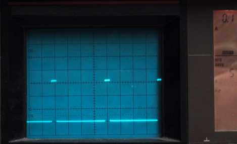
The input is a stream of pulses 5 volts high. The pulses are about 1ms long for OFF and 2mS long for ON. The actual length will vary depending on the make and model of your transmitter. The pulses shown here are the ON pulses at the input to the failsafe. |
 |

|
The pulses here are also at the input to the failsafe. This time they are failsafe OFF Note that the ON time for the pulse is now shorter |
|
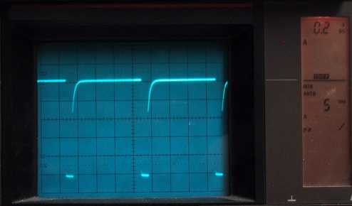
The collector of the first transitor, the 2N4401. The circuit has now inverted the pulses and increased their amplitude. The pulses shown are for the condition failsafe ON. |
 |
|
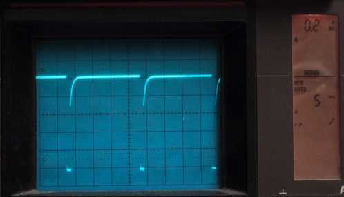
Again the collector of the first transitor, the 2N4401. This time the pulses are for failsafe OFF |
|
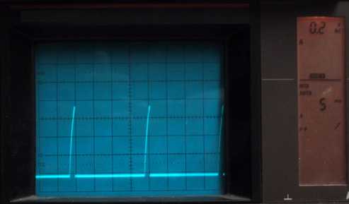
Pin 2 of the 555 timer. This pin is the trigger input of the chip. The pulses have now been differentiated. |
 |

|
Pin 3 of the 555 timer This is the output of the chip These are the reference pulses generated by the 555 timer. The pulses are always 1.5mS long These pulses should not vary in length. |
|
Pins 6 and 7 of the 555 timer. These pins are the timing pins of the chip. The waveform shown is the 555 timing the 1.5mS pulse. |
 |
|
|
Pin 5 of the 4013 D-Type flipflop This is the D input of the chip and should be the same as pin 3 of the 555 timer. These are the reference pulses generated by the 555 timer. The pulses are always 1.5mS long These pulses should not vary in length. |
|
Pin 3 of the 4013 D-Type flipflop. This is the Clock input of the chip and should be the same as the collector of the 2n4401 transistor. The waveform shown is the ON pulse. |
|
|
|
Pin 3 of the 4013 D-Type flipflop again This is the Clock input of the chip and should be the same as the collector of the 2n4401 transistor. The waveform shown is the OFF pulse |
|
Pin 6 of the 4013 D-Type flipflop. This is the SET input of the flipflop. In the absence of pulses this pin goes high and sets the output to failsafe. |
 |
|
|
|
Specifications The maximum input Voltage is limited by the 555 chip to 15 Volts The minimum input voltage is 5 Volts
The maximum switching Current also depends on the FET used |